Progress in Power Electronics with Beta-Gallium Oxide
Joint project “ForMikro-GoNext” with participation of IKZ and FBH successfully completed
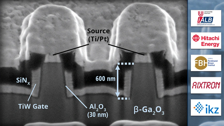
In the joint project “ForMikro-GoNext”, beta-gallium oxide (β-Ga₂O₃) was further developed as a pioneering semiconductor material for efficient power electronics. The partners made significant progress along the entire value chain, from volume crystal growth and epitaxy to device development and characterization. The material system was evaluated by demonstrating vertical transistors based on β-Ga₂O₃. The results of the project were examined by the industrial partners with regard to industrial utilization and indicate a high industrial relevance of the Ga₂O₃ technology. Utilization in the semiconductor and power electronics industry is therefore to be expected, which in turn strengthens Germany's technological sovereignty.
Our modern society relies on a multitude of electrical and electronic systems. Almost all of them require the conversion of one form of electricity into another in order to make the energy usable for us. According to a report by AG Energiebilanzen e.V., 65% of the energy generated in 2021 was lost mainly through power conversion, flare and line losses. Efficient power electronics are therefore essential and a decisive factor for the energy transition. As a new semiconductor material, beta-gallium oxide has the potential to reduce these conversion losses, cut costs and thus make a significant contribution to climate protection.
The joint project "ForMikro-GoNext" has advanced research on beta-gallium oxide from the basic research to the application level. In cooperation with the Leibniz-Institut für Kristallzüchtung (IKZ), the Ferdinand-Braun-Institut (FBH), the University of Bremen, and industrial partners Hitachi Energy and AIXTRON, the semiconductor material was studied in an innovative vertical component architecture to efficiently utilize its exceptional properties for transistors. Within the project, the entire process chain was further developed, achieving significant progress in material research (particularly in bulk crystal growth and epitaxy), device processing, and (material and device) characterization. The long-term stability of the material was also investigated. The result is clear: there are no physical limitations preventing the achievement of the theoretically predicted outstanding material properties, therefore the focus now lies on scaling the process. The results of GoNext lead the international status-quo and form an important cornerstone for Germany's technological sovereignty in the field of power electronics.
The joint project was funded by the Federal Ministry of Education and Research (BMBF) with around 2 million euros over 4 years (+1 year extension).
Contact:
Leibniz-Institut für Kristallzüchtung (IKZ)
Dr. Andreas Popp
+49 30 246499-312
andreas.popp(at)ikz-berlin.de
https://www.ikz-berlin.de
Press release IKZ, 13 December 2024
